Running graphics on STM32H7R7 & S7
This article addresses the specific architecture of the STM32H7R/S series MCUs and discusses the required considerations when using it for graphics. However, most of these considerations are applicable to all STM32 MCUs running graphics with external RAM and flash.
The article is not a beginner’s guide on how to create TouchGFX Board Setups (TBSs), as the STM32H7R/S is a high-performance and hence advanced MCU. Therefore, the article will also only dive into areas specific and important to STM32H7R/S. For a general introduction on how to create TouchGFX TBSs, refer to the Board Bring Up guide.
For more information on the STM32H7R7/S7 please visit the product page or the YouTube playlist containing a full STM32H7RS demo workshop.
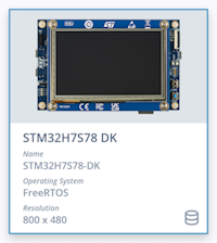
TouchGFX Designer contains a TBS for STM32H7S78 DK, which is a complete example project of running TouchGFX on STM32H7R/S. The TBS can be used as reference when developing a TouchGFX application for STM32H7R/S. The project is based on STM32CubeMX, which means the recommended configuration for cache, MPU, external memory, etc. can be accessed by opening the STM32H7S78-DK.ioc file.
Memory setup
STM32H7R/S is a bootflash MCU. A bootflash MCU is an MCU with a small embedded flash that contains the bootloader, while the main application is placed in external memory along with assets. STM32H7R/S also has 620 kB of embedded SRAM. As a result, STM32H7R/S relies on both external RAM and flash when used for graphics applications. When using external memories for graphics, the memory bandwidth to the external memories will often be the bottleneck since they run at half or a third of the CPU frequency. In the case of STM32H7R7/S7 the two XSPI (16 and 8 bit) interfaces can run at up to 200 MHz in double transfer rate and the FMC (16 or 32 bit) can run at up to 100 MHz.
External Memory Manager
Two tools called External Memory Manager and External Memory Loader are available from STM32CubeMX under Categories → Middleware and Software Packs. These tools are created to assist the user in setting up the external memories in bootflash or flashless applications. The tools make it easier to create external loaders and e.g. select application type. An introduction to the tools can be found here. A new article called ''Introduction to external serial memory with STM32'' will soon be published.
Framebuffers in external RAM
The first and most important thing to consider when having framebuffers in external RAM is the memory bandwidth requirements and constraints. With a display with no GRAM, it is required to continuously transfer the framebuffer at the specified rate by the display. For the displays used on the discovery kits, this is 60 Hz. This means that a lot of bandwidth on the external RAM interface will be occupied with only updating the LTDC. The required bandwidth by the LTDC can be calculated as follows:
pixel clock = LCD_CLK= total screen size * refresh rate
Required bandwith(for one LTDC layer) = LCD_CLK * Bpp
Furthermore, DMA2D and GPU2D will also require bandwidth on the external RAM when performing operations on the framebuffers. If the memory is also used for something else, such as application code, this will decrease the bandwidth even further.
Combined, these factors can clutter the external RAM bus.
An article explaining considerations when running graphics with framebuffers in external RAM can be found here.
For further information on constraints and considerations when having an LTDC display interface and framebuffers in external RAM, refer to the LTDC application note. Pay special attention to chapter 5: “Creating a graphical application with LTDC” and chapter 7: “LTDC application examples”.
If the bandwidth on the external RAM is at its limit, consider chapter 5.5.2: “Optimizing the LTDC framebuffer fetching from external memories” and chapter 5.5.3: “Optimizing the LTDC framebuffer fetching from SDRAM”.
Further reading
Tightly coupled memory
The STM32H7R/S Cortex-M7 features a 64-bit wide direct access to tightly coupled memories (TCM) with zero wait state. It has up to 192 kB of both data TCM (DTCM) and instruction TCM (ITCM). The DTCM and ITCM are hence the best locations for read/write of data and instruction fetch respectively. Therefore, the ITCM should be used for critical code with deterministic execution, such as interrupt handlers that cannot wait for cache misses, as well as e.g. critical control loops. In real-time applications that use RTOS, the heap is generally massively used. It is therefore recommended to place the RTOS stack and heap in DTCM. If there is any space left, global variables could be placed here as well.
It is important to note that ITCM and DTCM are using some parts of the SRAM1 and SRAM3 memories. This implies that the size of the internal SRAM will shrink when using ITCM and DTCM.
Like other H7 MCUs, STM32H7R/S has Level 1 (L1) cache. For more information on L1 cache, refer to the H7 cache application note. Pay special attention to chapter 4: “Mistakes to avoid and tips”.
For a detailed description of how to setup external SPI memories, refer to OSPI, HSPI and XSPI application note.
Further reading
Application type
During startup, the bootloader can do different things depending on the selected application type. It can either point to the application already in place in the external flash, or load the application to another memory, typically external RAM.
Executing the application already in place in external flash is called execute-in-place (XiP). Copying the application from flash to RAM during boot and then executing from RAM is called load-and-run (LRUN).
If the application is encrypted, it is only possible to use LRUN. For further information on encryption on STM32, refer to the application note on encryption.
Execute in Place (XiP)
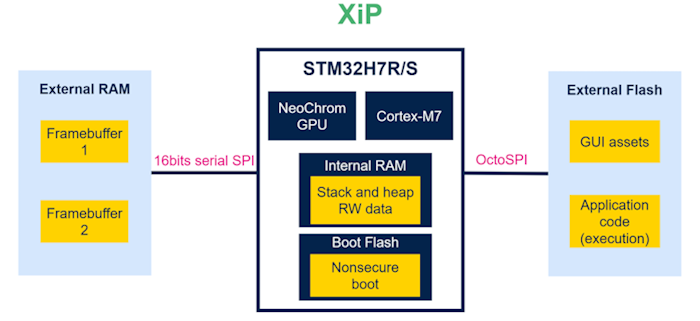
An example of how the memory layout for XiP could look like for a graphics application is illustrated below. XiP is the default application type.
As shown in the XiP illustration, the OctoSPI interface to the external flash is used to access both application code and graphics assets. The CPU constantly accesses the application code, which can lead to slower access times for NeoChrom GPU or Chrom-ART when accessing the assets. This will negatively impact graphics performance. To mitigate this challenge, it is highly recommended to enable the instruction cache for external flash when running XiP. By doing so, repeated instructions will be read from the cache instead of the external flash, thereby reducing the load on the bandwidth and increasing the efficiency of the external flash interface.
Load and Run (LRUN)
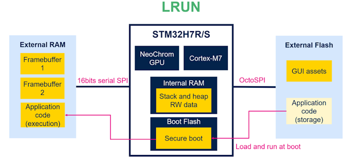
A corresponding example for LRUN is illustrated below.
As shown in the LRUN illustration, the application code is now separated from the graphics assets, which improves the access of assets. However, this also means that it is now the interface to the external RAM, which will be loaded, since it is needed to access both framebuffers and application code. In this case, it is highly recommended to enable instruction cache on the external RAM interface.
When using LRUN on STM32H7R/S with a graphics application, there are a few extra things to consider to achieve the best possible performance.
First, consider if the assets (bitmaps, fonts, etc.) could be kept in external flash. Since the assets are accessed frequently, storing them in external RAM will significantly load the bandwidth of the external RAM. Furthermore, it is typically unnecessary to encrypt assets.
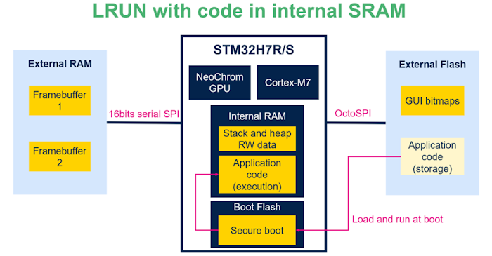
Secondly, it is worth investigating if the application code will fit in internal SRAM as illustrated below. The application code can be accessed and executed even faster from internal SRAM compared to having it in external flash or external RAM, as the internal buses are faster. The AXI bus on STM32H7R/S, to which the internal SRAM is connected, can run at speeds of up to 300 MHz. Furthermore, this configuration allows assets, framebuffers, and application code to be placed in three different locations, thereby distributing the bandwidth load across three separate buses.
Performance comparison
Below are examples of complex GUIs using XiP and LRUN respectively. The LRUN application has the application code in internal SRAM. The comparison shows how the MCU load is impacted by the different configurations. By placing the TouchGFX framework and application into the internal SRAM, the number of cycles for fetching in external RAM and flash is reduced, which effectively decreases the MCU load.
Demo reference is the out-of-box demo running on STM32H7S78-DK.
The comparison shows that the MCU load is reduced when the application code is placed in internal SRAM. The MCU load is reduced by approximately 50% when using LRUN compared to XiP.
The comparison shows that the MCU load is significantly reduced when the application code is placed in internal SRAM. This is due to the faster access times of the internal SRAM compared to external RAM and flash. The MCU load is reduced by 50% when using LRUN with the application code in internal SRAM compared to XiP. Using LRUN with application code stored in internal SRAM offers the best performance. However, this configuration is only feasible when the application code fits within the available internal SRAM.
MPU configuration
The memory protection unit (MPU) is used to protect memory areas from unintended memory access and -execution.
On Arm® Cortex®-M7 processors, it is important to prevent speculative access as it may cause high latency or system errors when performed on external memories. For STM32H7R/S, this will impact the AXI masters accessing the memories and it will significantly decrease graphics performance.
The MPU can be used to prevent speculative read access, by controlling the accessible address ranges. The easiest way to do this is by using a background region with the entire memory area, which restricts access by setting it to “strongly ordered, execute never”.
The background region should be defined in the default region with ID -1 since all other regions will then have priority over this region. Then, other MPU regions with respective settings should be defined for the memory areas that need access. It is possible to define up to 16 regions on STM32H7R/S.
The MPU configuration from the STM32H7S78 DK TBS is inserted below. This configuration can be used as reference.
| Region 0 | All | Note |
|---|---|---|
| Attribute | Value | |
| MPU Region Base Address | 0x0 | |
| MPU Region Size | 4 GB | Covers the entire memory area of the MCU |
| MPU SubRegion Disable | 0x0 | |
| MPU TEX field level | Level 0 | |
| MPU Access Permission | ALL ACCESS NOT PERMITTED | Restrict all access |
| MPU Instruction Access | DISABLE | |
| MPU Shareability Permission | ENABLE | |
| MPU Cacheable Permission | DISABLE | |
| MPU Bufferable Permission | DISABLE |
| Region 1 | External flash | Note |
|---|---|---|
| Attribute | Value | |
| MPU Region Base Address | 0x70000000 | Base address of XSPI2 (external flash) |
| MPU Region Size | 128 MB | 128 MBytes external flash on the board |
| MPU SubRegion Disable | 0x0 | |
| MPU TEX field level | Level 1 | |
| MPU Access Permission | ALL ACCESS PERMITTED | |
| MPU Instruction Access | DISABLE | |
| MPU Shareability Permission | DISABLE | |
| MPU Cacheable Permission | ENABLE | |
| MPU Bufferable Permission | ENABLE |
| Region 2 | External flash | Note |
|---|---|---|
| Attribute | Value | |
| MPU Region | Enabled | |
| MPU Region Base Address | 0x70000000 | Base address of XSPI2 (external flash) |
| MPU Region Size | 2 MB | Properties for the first 2 MB of the external flash, where application code is placed, is overwritten |
| MPU SubRegion Disable | 0x0 | |
| MPU TEX field level | Level 1 | |
| MPU Access Permission | ALL ACCESS PERMITTED | |
| MPU Instruction Access | ENABLE | |
| MPU Shareability Permission | DISABLE | |
| MPU Cacheable Permission | ENABLE | |
| MPU Bufferable Permission | ENABLE |
| Region 3 | External PSRAM | Note |
|---|---|---|
| Attribute | Value | |
| MPU Region Base Address | 0x90000000 | Base address of XSPI1 (external PSRAM) |
| MPU Region Size | 32 MB | 32 MBytes external PSRAM on the board |
| MPU SubRegion Disable | 0x0 | |
| MPU TEX field level | Level 1 | |
| MPU Access Permission | ALL ACCESS PERMITTED | |
| MPU Instruction Access | DISABLE | |
| MPU Shareability Permission | DISABLE | |
| MPU Cacheable Permission | DISABLE | |
| MPU Bufferable Permission | DISABLE |
| Region 4 | DTCM | Note |
|---|---|---|
| Attribute | Value | |
| MPU Region Base Address | 0x20000000 | Base address of DTCM |
| MPU Region Size | 64 kB | Default 64 kB of DTCM |
| MPU SubRegion Disable | 0x0 | |
| MPU TEX field level | Level 1 | |
| MPU Access Permission | ALL ACCESS PERMITTED | |
| MPU Instruction Access | DISABLE | |
| MPU Shareability Permission | DISABLE | |
| MPU Cacheable Permission | DISABLE | Disable caching on DTCM, since it does not yield performance increase |
| MPU Bufferable Permission | DISABLE |
| Region 5 | SRAM | Note |
|---|---|---|
| Attribute | Value | |
| MPU Region Base Address | 0x24000000 | Base address of SRAM1 |
| MPU Region Size | 512 kB | Covers SRAM1, SRAM2, SRAM3 and SRAM4 |
| MPU SubRegion Disable | 0x0 | |
| MPU TEX field level | Level 1 | |
| MPU Access Permission | ALL ACCESS PERMITTED | |
| MPU Instruction Access | DISABLE | |
| MPU Shareability Permission | ENABLE | |
| MPU Cacheable Permission | ENABLE | |
| MPU Bufferable Permission | ENABLE |
| Region 6 | GPU2D command list | Note |
|---|---|---|
| Attribute | Value | |
| MPU Region Base Address | 0x2406e000 | NeoChrom GPU command list is placed here |
| MPU Region Size | 16 kB | Default size of NeoChrom GPU command list when using TouchGFX (defined in nema_hal.c) |
| MPU SubRegion Disable | 0x0 | |
| MPU TEX field level | Level 0 | |
| MPU Access Permission | ALL ACCESS PERMITTED | |
| MPU Instruction Access | DISABLE | |
| MPU Shareability Permission | ENABLE | |
| MPU Cacheable Permission | DISABLE | Disable caching on command list |
| MPU Bufferable Permission | ENABLE |
For general graphics-specific MPU configuration tips, refer to chapter 5.6.2: “Configure the memory protection unit (MPU)” in the LTDC application note.
For further reference, see the MPU application note. Pay special attention to chapter 3: “Cortex-M0+/M3/M4/M7 memory types, registers and attributes” and chapter 6: “MPU setting example with STM32Cube HAL on Armv6 and Armv7 Architectures”.
Further reading
Debugging
The following guide to debugging STM32H7R/S in STM32CubeIDE is available in the readme in the TBS available in TouchGFX Designer.
Debugging the code in an IDE can be complex because of the Bootloader and Application structure of the TBS for STM32H7S78-DK. To step through the code of the TouchGFX application in STM32CubeIDE, follow these steps:
- Generate code in TouchGFX Designer
- Open the project in STM32CubeIDE
- Launch a debug session for the Boot project
- Wait for the compilation and flashing to complete
- Terminate the debug session (Ctrl + F2)
- Launch a debug session for the Appli project
- Wait for the compilation and flashing to complete
- Click Resume (F8)
- Press the black NRST button on the STM32H7S78-DK board
- The application is now at a break point at the first line of main() in the Appli project. If not, click Resume (F8) once more
- Proceed by e.g. clicking Resume (F8) or Step Over (F6)
For further information on debugging, refer to the wiki page on How to start with DA access on STM32H7RS.
Further reading
Conclusion and general recommendations for graphics applications
As explained above, there are several considerations to be made when developing a graphics application for STM32H7R/S. However, by keeping these considerations in mind, it is possible to achieve great graphics performance due to the fast CPU and the powerful GPU2D.
First of all, it is very important to be aware of the bandwidth on the external memory buses. This applies to all MCUs that are used with external RAM and flash, but it is especially crucial to consider due to the bootflash structure of STM32H7R/S.
The performance can be significantly increased by placing critical instructions and data in the ITCM and DTCM memory.
Enable the L1 instruction and data cache integrated into the Arm® Cortex®-M7 processor as this will boost the performance as well.
Choose whether to run either XiP or LRUN based on application requirements but remember to be aware of memory bandwidth. If the application code can fit in internal SRAM, LRUN will be the best performing.
It is important to avoid speculative read access as this will potentially decrease performance quite significantly. This is done by applying appropriate MPU configurations to all memory regions.


