2. CPU Running
Motivation
In this section we will make sure that the MCU core, internal RAM and flash are running at the desired clock speed.
TouchGFX can run on any MCU speeds, but a wrong clock configuration can lead to lower than necessary performance. Later in your board bring up you need to configure specific timing parameters, e.g. an I2C clock for the Touch Controller. This is impossible without ensuring that the MCU runs with the correct speed.
For STM32 microcontrollers you setup up a system clock. This clock is then divided down to generate the FCLK core clock and various peripheral clocks like APB1 peripheral clock.
Goal
The goal for this section is to modify your project to get the correct clock configuration. You should also verify that your internal RAM and flash are running at the expected speed.
Verification
Here are the verification points for this section:
| Verification Point | Rationale |
|---|---|
| SystemCoreClock variable's value is correct | The microcontroller is configured to run at the desired frequency. |
| Internal RAM is readable | The microcontroller has the expected amount of internal RAM, it is readable, and the speed is measured |
| Internal Flash is readable | The microcontroller has the expected amount of internal flash, it is readable, and the speed is measured |
| Caching is disabled | Running with caches disabled makes the system less complex and easier to understand. |
Prerequisites
The following are the prerequisites for this step:
- Information about the clock source on your hardware. It is common to use a crystal, but other solutions are also possible.
Do
We will now go through the steps of adjusting the clock configuration of our project to get the required MCU frequency. Afterwards we will discuss how to measure read speed of the internal flash.
System Clock
In STM32CubeMX click on the "Clock Configuration" tab. This gives you an overview of the clock tree for your specific MCU:
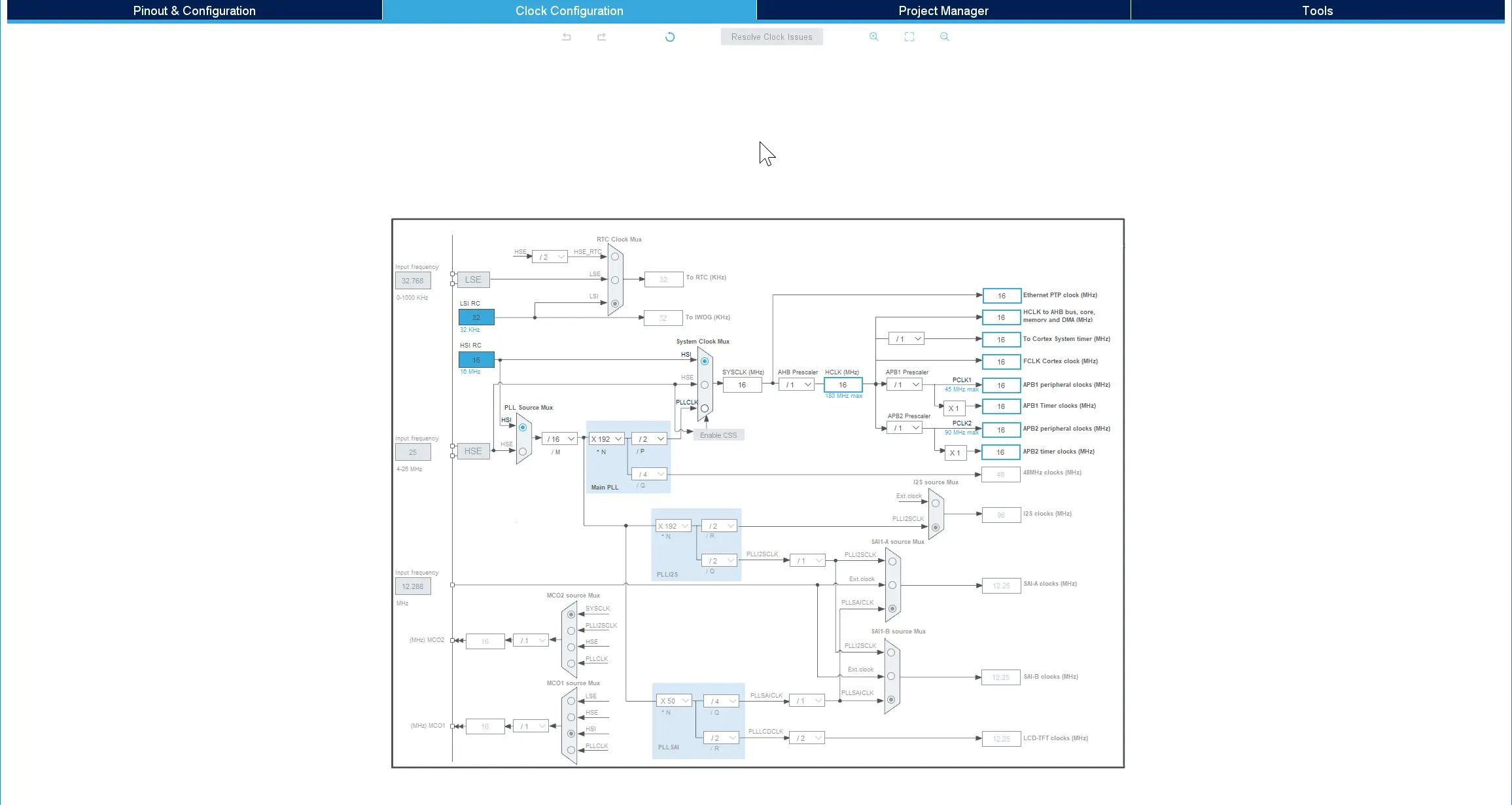
Clock Configuration
In this example the clock source is selected to be HSI. Many projects use an external crystal and must use HSE with a suitable divider (/M) and multiplier (/N). It is out the scope of this guide to advice on the clock configuration. After you have changed the clock configuration you must regenerate the project in STM32CubeMX (click Generate Code in upper right corner).
The core clock (HCLK) can be calculated at runtime by the generated code and saved in a variable. This variable can be used by application code to correctly convert between clock cycles and seconds, and e.g start timers. To get the variable recalculated you must call the SystemCoreClockUpdate() function. Insert a call in main.c (in a user code section):
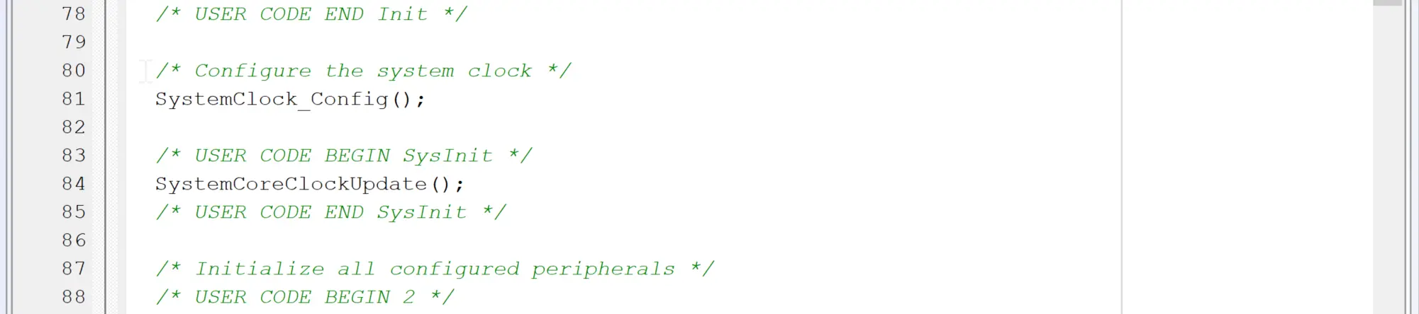
SystemCoreClockUpdate
If we set a breakpoint at the end of that function we can see the core clock (according to the configuration):
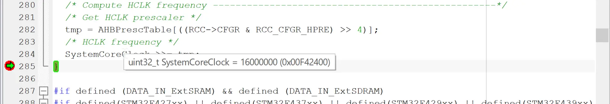
SystemCoreClock
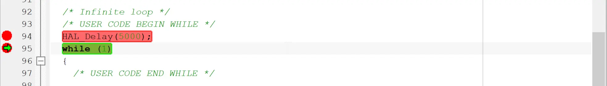
Another important point to test is the System Timer. This timer is running on HCLK divided down to give an interrupt every 1 ms. This timer is used by the STM32Cube Firmware to implement millisecond delays.
We can test this by inserting a delay of e.g 5 seconds in main. Verify this with a stop watch or similar means:
Measure delay
Flash and RAM size and speed
It is easy to check the reading speed of memory by using the System Timer. The System Timer interrupt increments a variable each millisecond. By reading this variable before and after a piece of code, we can measure the running time of the code (with 1 ms resolution). This scheme can be used to measure a time period in many different places in your application. It is not very precise, but can be done without external devices like oscilloscopes.
To do that we first need two volatile variable to save the result. If we don't save the result here, the optimizing compiler will in some case remove the measuring code:

Global volatile variables to hold measurement results
Here is an example where we read the flash from 0x08000000 to 0x08020000 (128 Kb) and time the code:
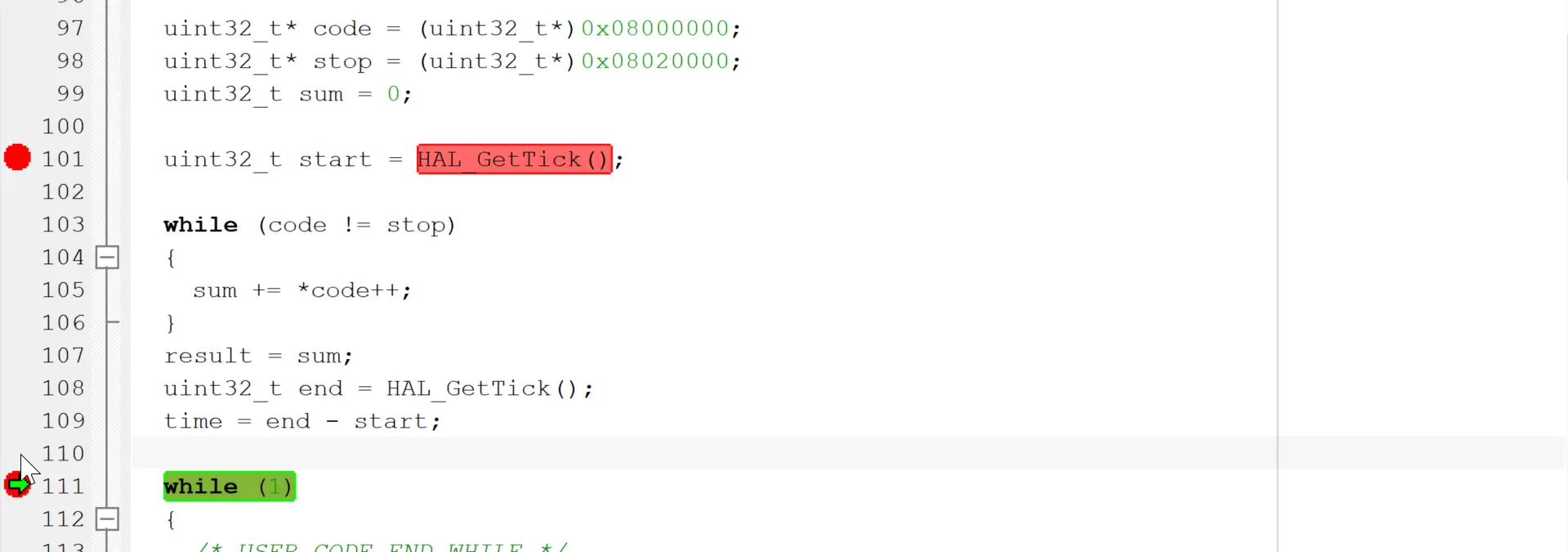
Timing a read loop
You can use code like this to verify the speed of your different memories. Once you have created a setup in STM32CubeMX you can measure the read speed and make a note of the result. The measurements can then be repeated later and verified. If you want to measure the bandwidth of your memory (the read speed in kb/s), you can compare the amount of data with the time measured.
On a 16 MHz STM32F429 the code runs in 12 ms giving us a read speed of the internal flash (using this method) of 128kb/0.012s = 10,666 kb/s.
The same loop above can easily be changed to verify that all the internal flash is enabled and readable. Just change the start and end addresses.
The code can also check the internal RAM. On the F429 the RAM starts at address 0x20000000. The core coupled memory is at 0x10000000. Check the datasheet for your specific MCU for the relevant memory addresses.
You should make a few measurements on your different memories and make a note of the result. For RAM test both the read and write speed.
Linker script
Another thing to look at is the linker script. This configuration file tells your linker what are the addresses of the RAM and flashes in your system. The linker script is generated by STM32CubeMX together with the project, but it can be good to study it. Later you will in most cases have to modify it to suit your project's needs.
Cache on F7 and H7
The ARM Cortex-M7 based STM32F7 and STM32H7 microcontrollers include data and instruction caches. It is recommended to disable at least the data cache until you have a stable platform. The data cache improves the performance significantly in many cases, but it also introduces complexity during testing.
When you have a stable platform, you can enable the data cache. It is easier at that point to identify that a given problem originates from data cache management, since the platform is otherwise functional.
The complexity of the data cache comes from the fact that the MCU core reads and writes to the cache, whereas peripherals like DMA2 and LTDC read directly from memory (and not in the cache). For this reason, you can be in a situation where you write data to e.g. your framebuffer, but some of the data is not seen on the display. This is because the LTDC did not find the new data in the RAM because it is only written to the cache so far. The solution is to flush the cache at certain points in your project, but we recommend to deal with this at a later point.
Caching can be disabled/enabled in STM32CubeMX in the System Core section.
TouchGFX internal DCache State Machine
TouchGFX engine keeps track of the current and last rendering operation, there are two states HARDWARE and SOFTWARE. The initial state is set to HARDWARE as the majority of draw operations are done by hardware. When a state switch occurs the state machine will call the appropriate virtual function to handle cache invalidation. When the state transit from HARDWARE to SOFTWARE it will call the virtual method void touchgfx::HAL::InvalidateCache() and when the state transitions from SOFTWARE to HARDWARE it will call the virtual method void touchgfx::HAL::FlushCache(). The functionality of these two functions is left for the user to implement in the derived HAL class.

TouchGFX engine internal DCache State Machine
If using TouchGFX Generator the implementation of these derived methods will be created in the TouchGFXGeneratedHAL class with function calls to DCache invalidation and no further action is needed.
Further Readings
The documents linked here contains more information about STM32CubeMX and the STM32 caches:
Further reading
- Section on Clock configuration in the STM32CubeMX User Manual
- Level 1 cache on STM32F7 and STM32H7