MCU
The microcontroller unit (MCU) is at the core of any embedded solution and there are a wide variety of options in terms of both cost and features.
When selecting an MCU for graphics, it is important to consider the supported display interfaces, the MCU package size, and the achievable graphics performance, which depends on two main factors:
图像合成
- MCU中集成的图形加速器的可用性。
- 系统中缓存存储器的可用性。
存储器存取和带宽
- 时钟频率和子系统总线频率。
- 对内部Flash和RAM存储器的存取。
It is also important to consider other aspects of the application, such as e.g. motor control or wireless communication, which run in addition to the graphics. These factors can influence the choice of MCU.
This page will explore the various MCU options and the parameters to consider when selecting an STM32 MCU for a GUI-driven application.
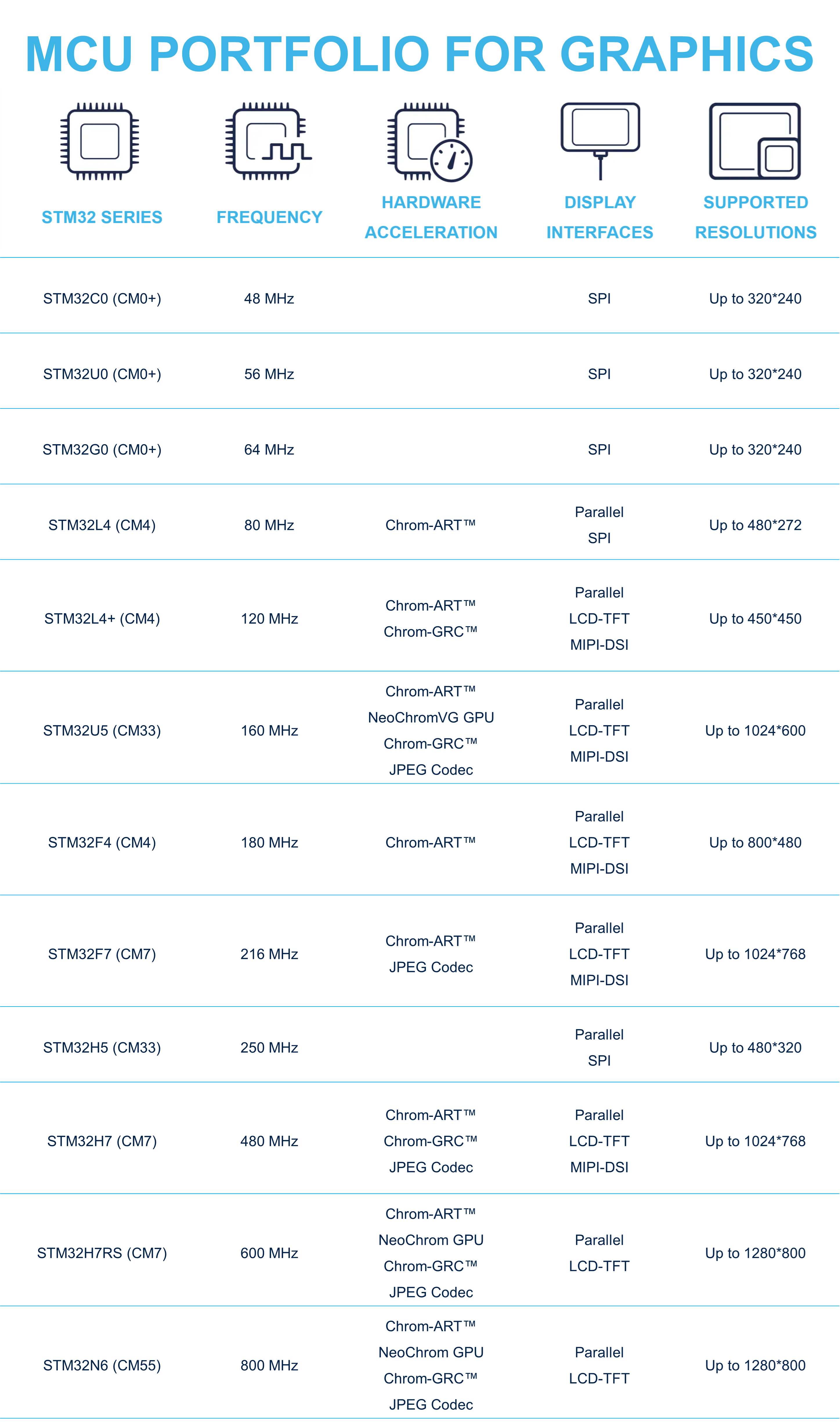
STM32 MCUs for graphics
For a complete overview of the STM32 MCUs listed above, including information about internal memory and peripherals, see the STM32 MCU portfolio.
Further reading
- The complete STM32 MCU portfolio can be found here.
- For a more complete overview of all product lines, including prices etc., the ST MCU Finder is available here.
频率
The core frequency has a major impact on the performance of a graphical application in terms of screen refresh, fluidity of screens, and animations.
它会影响可从内部或外部存储器传输到显示屏帧缓冲的大量数据,还可能影响计算和动画。
频率越高,在给定时间范围内能够传输的数据就越多,就能实现更复杂的动画。
The core frequency of STM32 MCUs is up to 800MHz.
Note
图形子系统频率
必须将内核CPU频率与图形子系统频率区别开来。 图形子系统频率包括内部总线频率和图形计数器频率,以及内部和外部存储器的存取速度。
图形子系统频率还会极大地影响整体图形性能。
An example of how to calculate the performance of a graphics subsystem can be found in this article. The article focuses on framebuffers in external RAM, but the same procedure can be applied to internal RAM as well.
嵌入式硬件加速功能
不同的STM32 MCU具有不同的内置硬件加速功能,有助于获得高性能的图形应用。
NeoChrom GPU
NeoChrom GPU can hardware accelerate some graphical operations such as texture mapping, scaling and vector rendering. It is also known as GPU2D.
NeoChrom GPU also comes in a version called NeoChromVG GPU, which can further accelerate vector rendering.
For a detailed description of NeoChrom GPU and its capabilities, visit the article about TouchGFX on NeoChrom/NeoChromVG.
Chrom-ART
Chrom-ART是一种先进的DMA,可以为执行图形操作提供辅助。 它也被称为DMA2D。
许多STM32平台中集成了Chrom-ART加速器,它能够控制和传输图像,而不会增加CPU负载。 它能够加快大多数图形操作的速度,如颜色填充、图像复制、混合和像素格式转换。
Chrom-ART加速器能够在一项操作中执行两个图层的混合,将初始像素格式转换为需要的输出像素格式,并将结果传输到存储器目标位置。
Chrom-ART加速器还支持有颜色查找表(CLUT)的颜色模式。 这有助于节省存储空间。
Example of an application running on the STM32F469-EVAL board where the CPU load is decreased from 82% to 4% when the Chrom-ART is enabled:
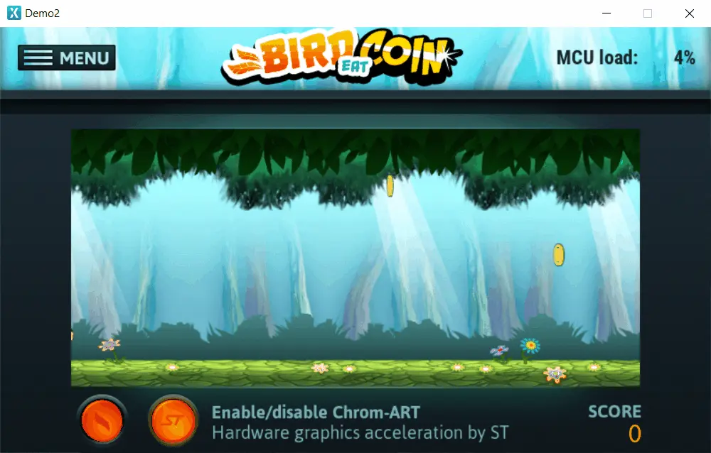
Bird-Eat-Coin Chrom-ART示例
此外,STM32H7产品为Chrom-ART外设增加了从YCbCr模式转换至RGB模式的能力。 此特性结合JPEG硬件编解码器,可减轻JPEG图像编码和解码时的CPU负载。
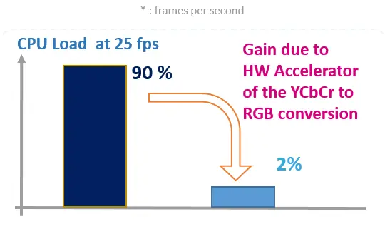
YCbCr转RGB硬件性能
具有上述特性的Chrom-ART加速器为图形应用提供了巨大优势。 TouchGFX(若选择的MCU中有提供)处理所有Chrom-ART特性,并将所有可能的绘图操作重定向至Chrom-ART外设而非CPU。
为高性能STM32系列提供了Chrom-ART外设。
Further reading
JPEG硬件编解码器
Some STM32 families provide a hardware JPEG codec to encode and decode images and videos.
如果UI应用需要播放视频文件或显示JPEG图像,则此特性十分重要。
JPEG图像占用的存储空间通常较小。 JPEG硬件编解码器确保在运行时间解码图像,而不会发生CPU超负载。
一些TouchGFX演示利用JPEG硬件编解码器,减轻播放MJPEG视频时的CPU负载。
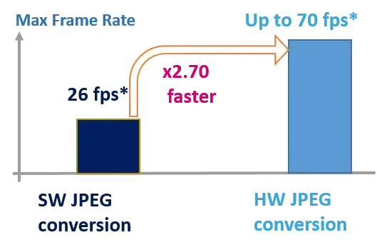
硬件JPEG编解码器性能
Further reading
Chrom-GRC
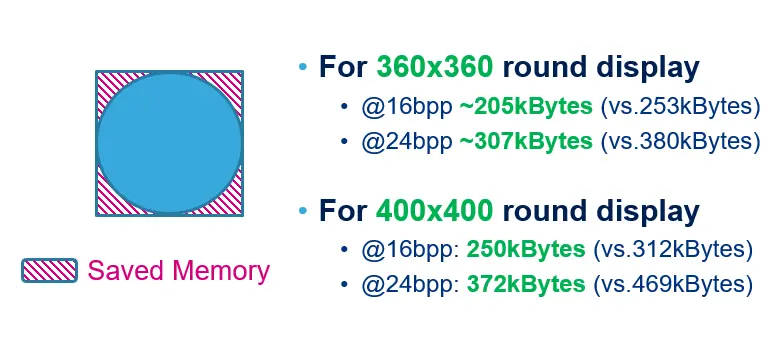
在一些STM32微控制器中,外设STM32 Chrom-GRC™(GFXMMU)旨在为向非矩形显示屏发展的新趋势提供高效支持。
在寻址非矩形显示屏时,Chrom-GRC™外设可帮助应用减少存储帧缓冲所需的RAM空间。
对于圆形显示屏,外设可将存储空间要求降低20%。
在控制非方形屏幕时,建议但不强制使用Chrom-GRC™外设。
Chrom-GRC™ is also utilized when using emulated framebuffer.
通过Chrom-GRC外设优化存储器
Further reading
内部Flash
使用位图资源的图形用户界面应用需要使用非易失性存储器来存储数据。 The execution from and access to internal flash is in some cases up to several times faster than external flash.
由于内部Flash的大小有限,很多时候会用内部Flash来存储TouchGFX框架、屏幕定义和UI逻辑,而位图数据则存储在外部Flash中。
The portfolio of STM32 products used for graphic applications is between 0 Kbytes and up to a few Mbytes of internal flash memory.
当位图数据量与内部Flash不匹配时,可能需要用到外部存储器。
Further reading
TouchGFX闪存要求:
- 框架:60 KB至100 KB。
- Screen definition and GUI logic: 1kbytes to 100kbytes.
这些数字取决于使用的框架特性,以及应用的大小和复杂度。
内部RAM
内部RAM可用于存储帧缓冲的前提是帧缓冲的大小使之能够放入可用存储器。 或者,也可以为设置增加外部存储器。
根据宽度、高度和色深计算帧缓冲的大小。 例如,对于具有HVGA分辨率(480x320)和16位色的显示屏,一个帧缓冲所需的存储空间为:
1个帧缓冲的大小 = 480 x 320 x 2 = 307,200字节
对图形应用使用的STM32产品的内部RAM大小介于几KB和几MB之间。
Further reading
TouchGFX RAM要求:
- 框架:10 KB至30 KB
- 控件:1 KB至15 KB
不同应用的存储空间要求可能不同。
LCD控制器
MCU的选择还取决于要使用的显示屏接口和分辨率。 以800x480的分辨率为例,只能通过数据传输足够高效的接口来实现。 RGB-TFT和MPI-DSI接口通常用于更高分辨率,原因是在许多情况下,带宽高于SPI或并行8080/6800。 低分辨率显示屏通常内置控制器和GRAM,可通过简单的SPI或8080/6800接口进行连接。
高分辨率显示屏(WQVGA及以上)通常没有内置控制器和GRAM,因此控制器需位于微控制器侧。 STM32 MCU内置了RGB-TFT和MIPI DSI接口的控制器。
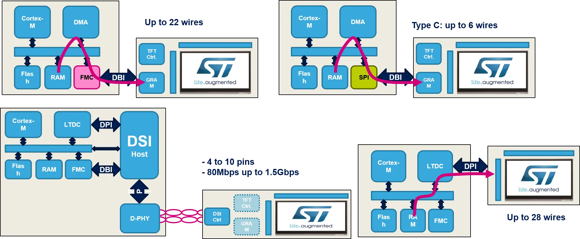
图中显示了有/没有GRAM和显示屏控制器的不同显示屏接口的4个示例。
Further reading
封装& I/O
需要的I/O数量取决于选择的显示屏和外部存储器。 运行具有并行RAM/Flash的并行显示屏可能需要大量I/O,导致封装尺寸变大。
存储器接口
当微控制器中的内部闪存和RAM不够用时,选择具有最合适外部存储器接口的合适MCU就变得十分重要。 STM32产品提供了不同的存储器控制器外设,用于连接NOR、NAND、SRAM、SDRAM、LPSDR SDRAM和PSRAM存储器。
可变存储控制器& 可变静态存储控制器(FMC/FSMC)
除了支持静态RAM,FMC还为FSMC增加了动态RAM支持(SDRAM)。 The flexible memory controller (FMC) with its high external access speed and up to 32 bit data bus, allows for higher throughout from and to external RAM and hence better support of higher resolution. FMC的每个存储区有独立的芯片选择。 FMC可以控制用于数据的外部Flash、用于帧缓冲的外部RAM存储器和用于图形栈的堆扩展。
串行存储器接口
Depending on the STM32 product, the serial memory interface is embedded and allows interfacing with single, double, quad, octo, and HyperBus™ flash memories alongside QSPI, PSRAM, OPI PSRAM, and Hyper RAM memories. The serial high speed memory interface can control up to 256Mbytes when in memory mapped mode and 4Gbytes in indirect mode.
相比于并行接口,串行存储器接口可将成本较低的外部闪存连接到小型封装,同时减少使用的引脚数。
However, the efficiency is usually lower with serial flash memory compared to parallel flash memory.
Further reading
Cortex®-M Core
STM32 MCU采用不同的ARC Cortex®-M架构。 下面是STM32上运行图形时最常用的内核。
Cortex®-M0+
Cortex®-M0+的特点在于它架构简单且价格低廉。 建议将其应用于以较低分辨率运行的较小的静态图形应用。
Cortex®-M4
与M0+相比,Cortex®-M4包含更多功能,并加快了计算速度。 它包含DSP指令集和单精度FPU单元。 这些指令可减轻CPU负载并提高计算速度。
Cortex®-M7
Cortex®-M7包含更复杂的架构,也包含DSP指令集,并具有更高效的双精度FPU单元,以及可容纳最多16KB的数据和指令的一级缓冲存储器。 缓冲存储器提供了使数据和指令紧邻计算单元以便优化提取时间的可能性。
Cortex®-M33
The Cortex®-M33 is a core with advanced security features. It includes TrustZone® technology, which allows the MCU to run secure and non-secure applications on the same core. It has a simpler architecture compared to the CM7.
Cortex®-M55
The Cortex®-M55 is designed for AI and DSP applications and includes Helium technology for vector processing. The CM55 also includes TrustZone® technology.
特性概述
| 特性 | Cortex-M0+ | Cortex-M4 | Cortex-M7 | Cortex-M33 | Cortex-M55 |
|---|---|---|---|---|---|
| DMIPS/MHz范围 | 0.95-1.36 | 1.25-1.95 | 2.14-3.23 | 1.54 | 1.69 |
| Core Mark®/MHz | 2.46 | 3.42 | 5.01 | 4.10 | 4.40 |
| 数字信号处理(DSP)扩展 | 无 | 有 | 有 | 有 | 有 |
| 浮点硬件 | 无 | 有(SP) | Yes (SP, DP) | 有(SP) | Yes (SP, DP, HP) |
| 内置缓存 | 无 | 无 | Yes (option 4-64kB), I-Cache, D-Cache | 无 | Yes (option 4-64kB), I-Cache, D-Cache |
| 总线协议 | AHB Lite,Fast I/O | AHB Lite,APB | AXI4,AHB Lite,APB,TCM | AHB, AHB Lite, APB | AXI, AHB, AHB Lite, APB, TCM |
| 双核锁步支持 | 无 | 无 | 有 | 无 | 有 |
For further reference, check the ARM Cortex-M Processor Comparison Table.
Level 1 cache
STM32H7和STM32F7系列包含最大16 KB的一级缓存,用于指令和数据缓存。 一级缓存在CPU附近保存了数据或指令集,因此CPU无需不断地提取重复使用的同一数据。
Further reading
双核
STM32H7系列包含双核系列:
Arm® Cortex®-M7和Cortex®-M4内核的运行频率分别可达到480 MHz和240 MHz,可以支持更多的处理和应用程序分区。 双核STM32H7产品系列可与嵌入式SMPS一起使用,以提高动态电源效率。
第二个Cortex®-M4可以减轻计算量,以便开放M7内核用于绘图/图形操作。
Note
总线架构
大多数STM32微控制器提供32位多AHB总线矩阵,用于互连所有主设备(CPU、DMA等)和从设备(Flash、RAM、FSMC、AHB和APB外设)。 这样一来,即使多个高速外设同时工作,也能确保无缝、高效的操作。
In addition to multi-AHB interconnect, some STM32 products embed 64-bit AXI to expand bandwidth. 因此,在性能和功耗之间实现了最佳平衡。
价格
内部Flash和内部RAM的大小以及封装中的可用引脚数都会影响MCU的价格。 用户可以根据接口、分辨率和性能等方面的要求,最终找到合适的MCU和估价。