MCU
The microcontroller unit (MCU) is at the core of any embedded solution and there are a wide variety of options in terms of both cost and features.
When selecting an MCU for graphics, it is important to consider the supported display interfaces, the MCU package size, and the achievable graphics performance, which depends on two main factors:
圖像合成
- MCU中集成的圖形加速器的可用性。
- 系統中緩存記憶體的可用性。
記憶體存取和頻寬
- 時脈頻率和子系統匯流排頻率
- 對內部快閃記憶體和RAM記憶體的存取。
It is also important to consider other aspects of the application, such as e.g. motor control or wireless communication, which run in addition to the graphics. These factors can influence the choice of MCU.
This page will explore the various MCU options and the parameters to consider when selecting an STM32 MCU for a GUI-driven application.
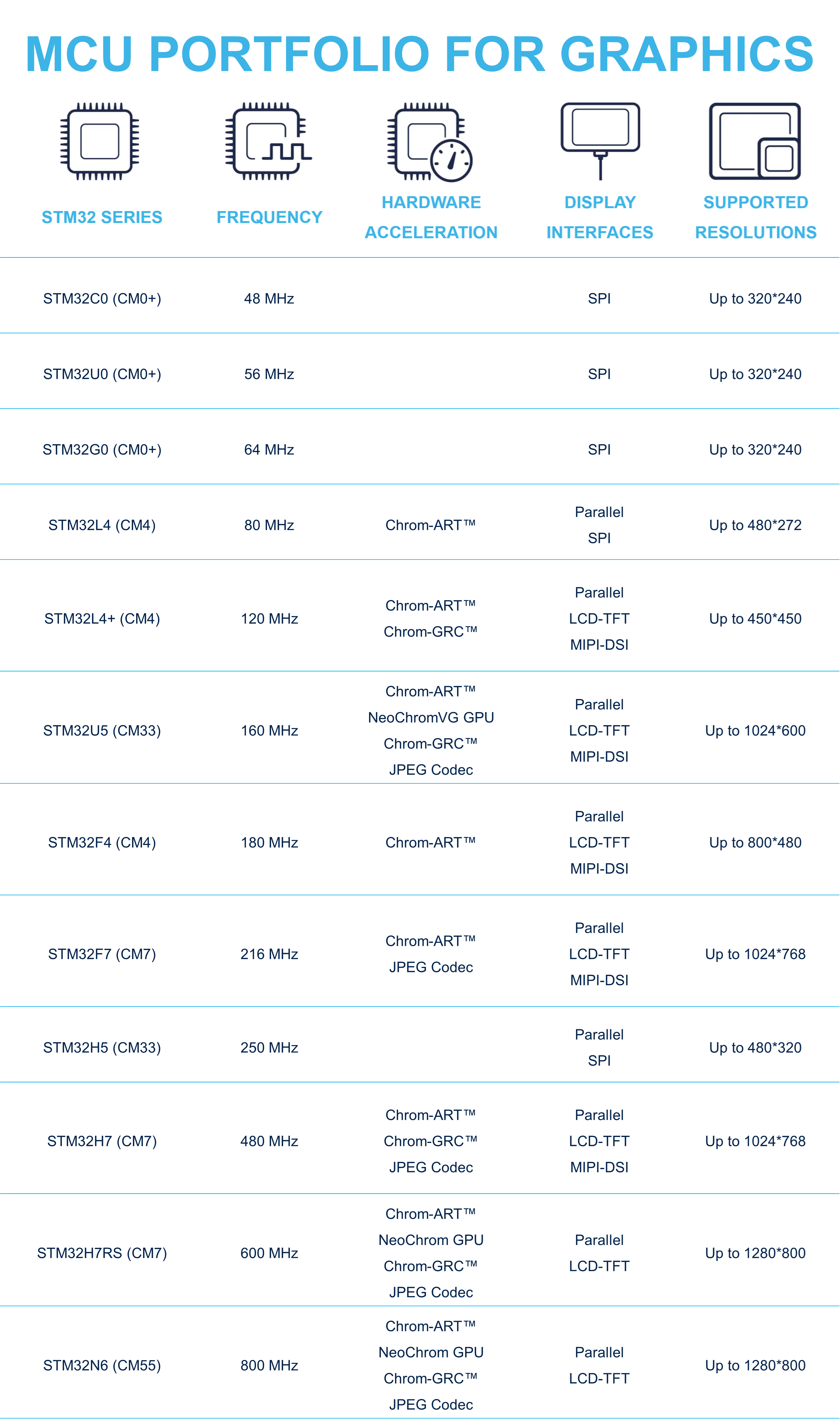
STM32 MCUs for graphics
For a complete overview of the STM32 MCUs listed above, including information about internal memory and peripherals, see the STM32 MCU portfolio.
Further reading
- The complete STM32 MCU portfolio can be found here.
- For a more complete overview of all product lines, including prices etc., the ST MCU Finder is available here.
頻率
The core frequency has a major impact on the performance of a graphical application in terms of screen refresh, fluidity of screens, and animations.
它會影響從內部或外部記憶體傳輸到顯示器影像緩衝的大量資料,還可能影響計算和動畫。
頻率越高,在特定時間範圍內能夠傳輸的資料就越多,就能實現更複雜的動畫。
The core frequency of STM32 MCUs is up to 800MHz.
Note
圖形子系統頻率
必須將核心CPU頻率與圖形子系統頻率區別開來。 圖形子系統頻率包括內部匯流排頻率和圖形加速器頻率,以及內部和外部記憶體的存取速度。
圖形子系統頻率還會劇烈地影響整體圖形性能。
An example of how to calculate the performance of a graphics subsystem can be found in this article. The article focuses on framebuffers in external RAM, but the same procedure can be applied to internal RAM as well.
嵌入式硬體加速功能
不同的STM32 MCU具有不同的內置硬體加速功能,有助於獲得高性能的圖形應用。
NeoChrom GPU
NeoChrom GPU can hardware accelerate some graphical operations such as texture mapping, scaling and vector rendering. It is also known as GPU2D.
NeoChrom GPU also comes in a version called NeoChromVG GPU, which can further accelerate vector rendering.
For a detailed description of NeoChrom GPU and its capabilities, visit the article about TouchGFX on NeoChrom/NeoChromVG.
Chrom-ART
Chrom-ART是一種先進的DMA,可以為執行圖形操作提供輔助。 它也被稱為DMA2D。
許多STM32平臺中集成了Chrom-ART加速器,它能夠控制和傳輸圖像,而不會增加CPU負載。 它能夠加快大多數圖形操作的速度,如顏色填充、圖像複製、混合和像素格式轉換。
Chrom-ART加速器能夠在一項操作中執行兩個圖層的混合,並將初始像素格式轉換為需要的輸出像素格式,並將結果傳輸到記憶體目標位置。
Chrom-ART加速器還支援有顏色查閱資料表(CLUT)的顏色模式。 這有助於節省存儲空間。
Example of an application running on the STM32F469-EVAL board where the CPU load is decreased from 82% to 4% when the Chrom-ART is enabled:
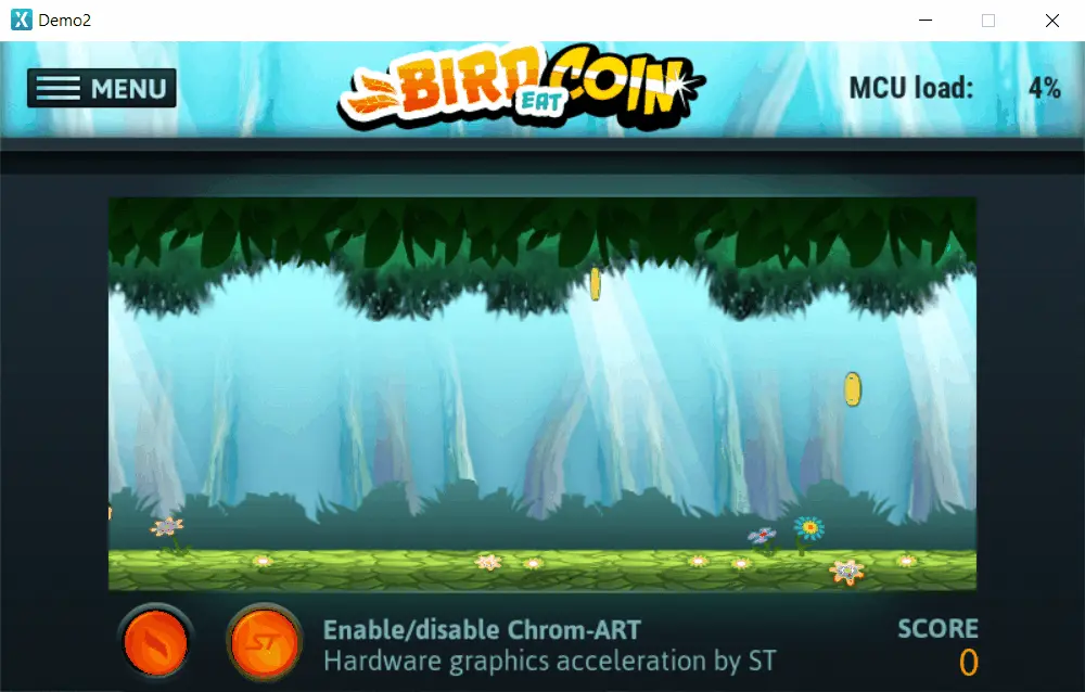
Bird-Eat-Coin Chrom-ART範例
此外,STM32H7產品為Chrom-ART外設增加了從YCbCr 模式轉換至RGB模式的能力。 此特性結合JPEG硬體轉碼器,可減輕JPEG圖像編碼和解碼時的CPU負載。
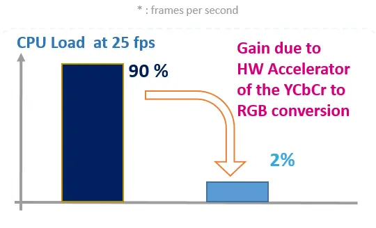
YCbCr轉RGB硬體性能
具有上述特性的Chrom-ART加速器為圖形應用提供了巨大優勢。 TouchGFX(若選擇的MCU中有提供)處理所有Chrom-ART特性,並將所有可能的繪圖操作重定向至Chrom-ART外設而非CPU。
為高性能STM32系列提供了Chrom-ART外設。
Further reading
JPEG硬體轉碼器
Some STM32 families provide a hardware JPEG codec to encode and decode images and videos.
如果UI應用需要播放影片檔或顯示JPEG圖像,則此特性十分重要。
JPEG圖像佔用的存儲空間通常較小。 JPEG硬體轉碼器確保在執行時間解碼圖像,而不會發生CPU超載。
一些TouchGFX演示利用JPEG硬體轉碼器,減輕播放MJPEG影片時的CPU負載。
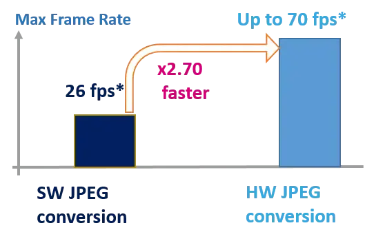
硬體JPEG轉碼器性能
Further reading
Chrom-GRC
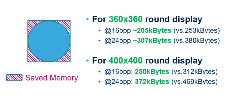
在一些STM32微控制器中,外設STM32 Chrom-GRC™(GFXMMU)旨在為向非矩形顯示器發展的新趨勢提供高效支援。
在定址非矩形顯示器時,Chrom-GRC™外設可減少存儲影像緩衝所需的RAM空間。
對於圓形顯示器,外設可將存儲空間要求降低20%。
在控制非方形螢幕時,建議但不強制使用Chrom-GRC™外設。
Chrom-GRC™ is also utilized when using emulated framebuffer.
通過Chrom-GRC外設優化記憶體
Further reading
內部快閃記憶體
使用點陣圖資源的圖形化使用者介面應用需要使用非揮發性記憶體來存儲資料。 The execution from and access to internal flash is in some cases up to several times faster than external flash.
由於內部快閃記憶體的大小有限,很多時候會用內部快閃記憶體來存儲TouchGFX框架、螢幕定義和UI邏輯,而點陣圖資料則存儲在外部快閃記憶體中。
The portfolio of STM32 products used for graphic applications is between 0 Kbytes and up to a few Mbytes of internal flash memory.
當點陣圖資料量與內部快閃記憶體不匹配時,可能需要用到外部記憶體。
Further reading
TouchGFX快閃記憶體要求:
- 框架: 60 KB 至 100 KB。
- Screen definition and GUI logic: 1kbytes to 100kbytes.
這些數位取決於使用的框架特性,以及應用的大小和複雜度。
內部RAM
內部RAM可用於存儲影像緩衝的前提是儲影緩衝的大小能夠放入可用記憶體。 或者,也可以為設置增加外部記憶體。
根據寬度、高度和色深計算影像緩衝的大小。 例如,對於具有HVGA解析度(480x320)和16位色的顯示器,一個影像緩衝所需的存儲空間為:
1個影像緩衝區的大小 = 480 x 320 x 2 = 307,200位元組
對圖形應用使用的STM32產品的內部RAM大小介於幾KB和幾MB之間。
Further reading
TouchGFX RAM要求:
- 框架: 10 KB至30 KB
- 小部件: 1 KB 至 15 KB
不同應用的存儲空間要求可能不同。
LCD控制器
MCU的選擇還取決於要使用的顯示器介面和解析度。 以800x480的解析度為例,只能通過高效的資料傳輸足夠介面來實現。 RGB-TFT和MPI-DSI介面通常用於更高解析度,原因是在許多情況下,頻寬高於SPI或平行8080/6800。 低解析度顯示器通常內置控制器和GRAM,可通過簡單的SPI或8080/6800介面進行連接。
高解析度顯示器(WQVGA及以上)通常沒有內置控制器和GRAM,因此控制器需位於微控制器側。 內置RGB-TFT和MIPI DSI介面的STM32 MCU上有控制器。
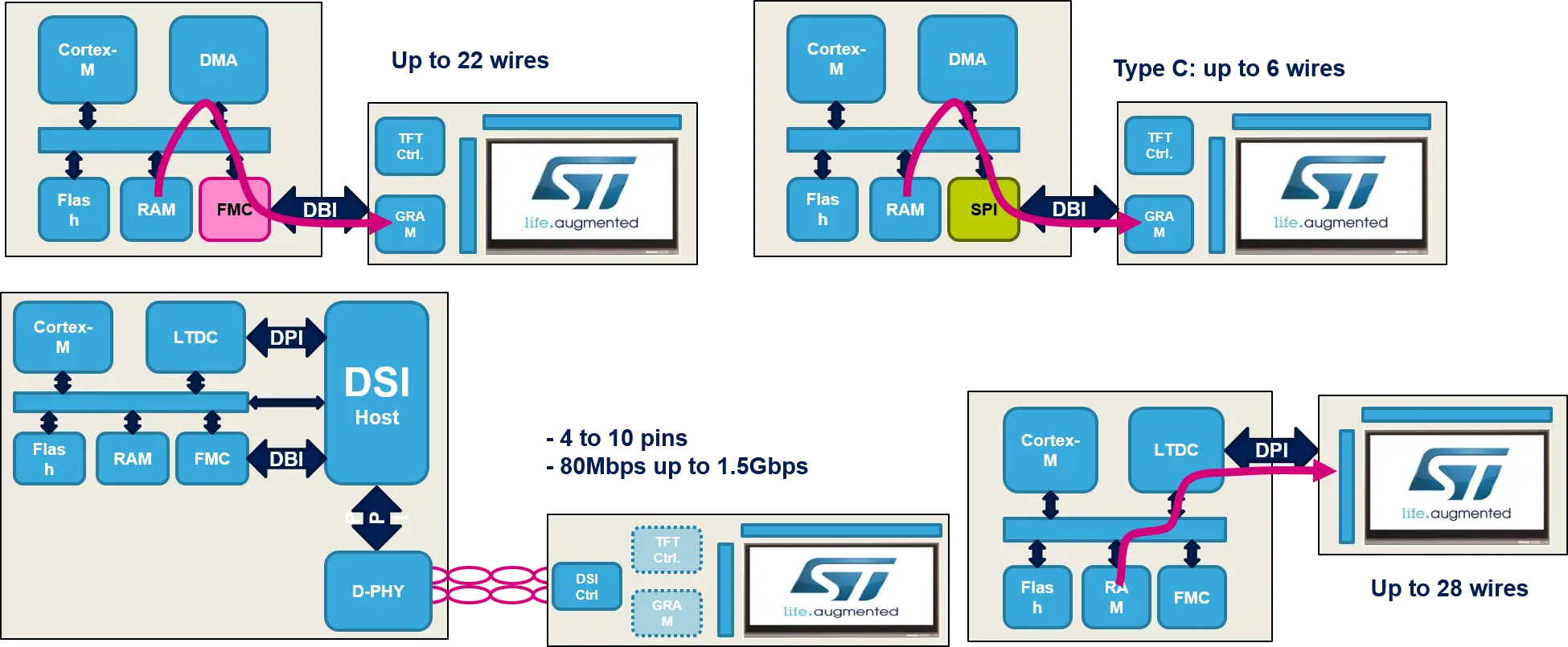
圖中顯示了有/沒有GRAM和顯示器控制器的不同顯示器介面的4個範例。
Further reading
封裝和I/O
需要的I/O數量取決於選擇的顯示器和外部記憶體。 運行具有平行RAM和快閃記憶體的平行顯示器可能需要大量I/O,導致封裝尺寸變大。
記憶體介面
當微控制器中的內部快閃記憶體和RAM不夠用時,選擇具有最合適外部記憶體介面的合適MCU就變得十分重要。 STM32產品提供了不同的記憶體控制器外設,用於連接NOR、NAND、SRAM、SDRAM、LPSDR SDRAM和PSRAM記憶體。
可變存儲控制器 & 可變靜態存儲控制器(FMC/FSMC)
除了支援靜態RAM,FMC還為FSMC增加了動態RAM支援(SDRAM)。 The flexible memory controller (FMC) with its high external access speed and up to 32 bit data bus, allows for higher throughout from and to external RAM and hence better support of higher resolution. FMC的每個存儲區有獨立的晶片選擇。 FMC可以控制用於資料的外部快閃記憶體、用於幀緩衝的外部RAM記憶體和用於圖形棧的堆擴展。
串列記憶體介面
Depending on the STM32 product, the serial memory interface is embedded and allows interfacing with single, double, quad, octo, and HyperBus™ flash memories alongside QSPI, PSRAM, OPI PSRAM, and Hyper RAM memories. The serial high speed memory interface can control up to 256Mbytes when in memory mapped mode and 4Gbytes in indirect mode.
相比於平行介面,串列記憶體介面可將成本較低的外部快閃記憶體連接到小型封裝,同時減少使用的引腳數。
However, the efficiency is usually lower with serial flash memory compared to parallel flash memory.
Further reading
Cortex®-M Cores
STM32 MCU採用不同的ARC Cortex®-M架構。 下面是STM32上運行圖形時最常用的內核。
Cortex®-M0+
Cortex®-M0+的特點在於它架構簡單且價格低廉。 建議將其應用於以較低解析度運行的較小的靜態圖形應用。
Cortex®-M4
與Cortex®-M4相比,M0+包含更多功能,並加快了計算速度。 它包含DSP指令集和單精確度FPU單元。 這些指令可減輕CPU負載並提高計算速度。
Cortex®-M7
Cortex®-M7包含更複雜的架構,也包含DSP指令集,並具有更高效的雙精度FPU單元,以及可容納最多16KB的資料和指令的一級緩衝記憶體。 緩衝記憶體提供了使資料和指令緊鄰計算單元以便優化提取時間的可能性。
Cortex®-M33
The Cortex®-M33 is a core with advanced security features. It includes TrustZone® technology, which allows the MCU to run secure and non-secure applications on the same core. It has a simpler architecture compared to the CM7.
Cortex®-M55
The Cortex®-M55 is designed for AI and DSP applications and includes Helium technology for vector processing. The CM55 also includes TrustZone® technology.
特性概述
| 特徵 | Cortex-M0+ | Cortex-M4 | Cortex-M7 | Cortex-M33 | Cortex-M55 |
|---|---|---|---|---|---|
| DMIPS/MHz範圍 | 0.95-1.36 | 1.25-1.95 | 2.14-3.23 | 1.54 | 1.69 |
| Core Mark®/MHz | 2.46 | 3.42 | 5.01 | 4.10 | 4.40 |
| 數位信號處理(DSP)擴展 | 無 | 有 | 有 | 有 | 有 |
| 浮點數硬體 | 無 | 有(SP) | Yes (SP, DP) | 有(SP) | Yes (SP, DP, HP) |
| 內置緩存 | 無 | 無 | Yes (option 4-64kB), I-Cache, D-Cache | 無 | Yes (option 4-64kB), I-Cache, D-Cache |
| 匯流排協定 | AHB Lite,Fast I/O | AHB Lite, APB | AXI4,AHB Lite,APB,TCM | AHB, AHB Lite, APB | AXI, AHB, AHB Lite, APB, TCM |
| 雙核鎖步支持 | 無 | 無 | 有 | 無 | 有 |
For further reference, check the ARM Cortex-M Processor Comparison Table.
Level 1 cache
STM32H7和STM32F7系列包含最大16 KB的一級緩存,用於指令和資料緩存。 一級緩存在CPU附近保存了資料或指令集,因此CPU無需不斷地提取重複使用的同一資料。
Further reading
雙核
STM32H7系列包含雙核系列:
Arm® Cortex®-M7和Cortex®-M4內核的運行頻率分別可達到480 MHz和240 MHz,可以支援更多的處理和應用程式分區。 雙核STM32H7產品系列可與嵌入式SMPS一起使用,以提高動態電源效率。
第二個Cortex®-M4可以減輕計算量,以便開放M7內核用於繪圖/圖形操作。
Note
匯流排架構
大多數STM32微控制器提供 32位元多AHB 匯流排矩陣,用於互連所有主設備(CPU、DMA等)和從設備(快閃記憶體、RAM、FSMC、AHB和APB外設)。 這樣一來,即使多個高速外設同時工作,也能確保無縫、高效的操作。
In addition to multi-AHB interconnect, some STM32 products embed 64-bit AXI to expand bandwidth. 因此,在性能和功耗之間實現了最佳平衡。
價格
內部快閃記憶體和內部RAM的大小以及封裝中的可用引腳數都會影響MCU的價格。 使用者可以根據介面、解析度和性能等方面的要求,最終找到合適的MCU和估價。